Design and Manufacturing Capability
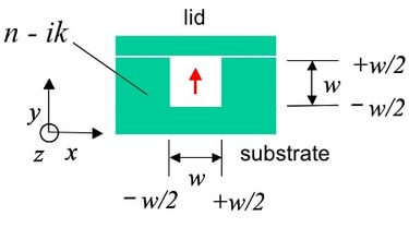
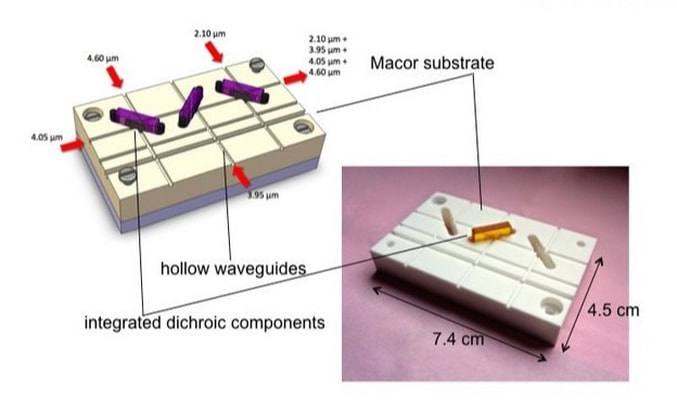
HollowGuide Ltd provides a design and manufacturing capability which enables customers to convert their new optical circuit concepts, or their existing free-space designs, into compact, rugged, high performance integrated optic systems. In practice the manufacturing approach utilises precision CNC milling (or alternative etching or 3D printing techniques) to create alignment features for discrete components in the surface of a dielectric substrate. Light is then guided through the circuit of components via hollow waveguides. The hollow waveguides are created in the surface of the substrate as square section channels in conjunction with a lid - which forms the forth upper wall of all the waveguides. Compared with solid core waveguides or optical fibres hollow waveguides have very broad waveband high power transmission characteristics making the applicable to a very wide range of applications.
Assembly of a hollow waveguide integrated optic circuit simply requires the location of the discrete optical components in their associated alignment features. In this manner the requirement for complex, sensitive and expensive alignment mounts, and costly time consuming manual alignment techniques is circumvented. Light guidance between the circuit components also significantly eases otherwise demanding angular alignment tolerances. The approach leads to high performance, compact, rugged, optical systems which are mechanically and optically robust in harsh environments. The approach lends itself to automated assembly processes leading to low cost, quality controlled, mass production. Whether for basic research, a development prototype or a commercial product, HollowGuide Ltd works with customers to carry their optical circuit concepts into high performance, compact, rugged systems.
Design Considerations
The design of an efficient hollow waveguide circuit depends on a number of factors. A major consideration is the operational wavelength. At any given wavelength the magnitude of the hollow waveguide attenuation coefficient can be made suitable small by appropriate choices of the complex refractive index of the substrate material (i.e. the walls of the hollow waveguides) and the hollow waveguide cross-section. However, the choice of waveguide cross-section also dictates the angular and lateral alignment tolerances that need to be achieved in practice in order that high fidelity fundamental mode propagation can be achieved through what are essentially multimode waveguides. Furthermore, the waveguide cross-section also defines the power density on the integrated discrete components. In practice the various trade-offs between the different design parameters are addressed in the design phase. With this phase completed a full engineering drawing for the hollow waveguide circuit is produced. If CNC milling techniques are to be used for manufacture the associated STEP (.stp) files form the basis of the CNC milling program.


