HollowGuide Ltd - Optical System Design
[email protected] +44 (0)7833 718 602 +44 (0)1684 574 738
Hollow waveguide optical PCB implementation of a 2.1 μm Differential Absorption Lidar (DIAL) demonstrator. The optical components are located in precision alignment features formed in the surface of a dielectric substrate and light is guided between the components in hollow waveguides. The hollow waveguides are created as square sectioned channels in the surface of the substrate - a lid, which sits on top of the substrate, acts as the fourth upper wall of all the waveguides. Optical guidance eases demanding angular alignment tolerances leading to significantly improved system performance while component integration circumvents the need for bulky and mechanically sensitive mounts leading to a more compact solution with greater robustness to misalignment in the field. The work was funded by the Centre for Earth Observation Instrumentation (CEOI).
What HollowGuide Ltd Provides
HollowGuide Ltd provides customers with a fundamentally new approach to optical system design and manufacture. The approach leads to significant practical advantages in terms of:
- reduced size and weight.
- increased ruggedness and optical stability.
- improved optical performance and reliability in the field.
- low cost, quality controlled, mass manufacture.
The systems design and manufacturing concepts are simple to implement, and are applicable to a wide range of optical and laser systems over a very broad waveband range. The concepts are readily applied to both one-off research prototypes and to low cost, mass-production of fully developed solutions. Application areas include:
- laser radar (Lidar)
- atmospheric, planetary and environmental sensing systems
- interferometers of all forms: Michelson interferometer, Fourier transform interferometer, etc
- laser heterodyne radiometers
- optical counter-measures (DIRCM)
- target marking
- beam multiplexers and demultiplexers
- laser and amplifier cavity design
- substrate integrated Hollow Waveguide Systems (iHWG).
Examples Optical and Laser Systems
A range of optical and laser configurations, where the concept has been successfully applied for different customers in different applications areas, are shown below with brief descriptions.
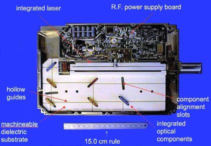
A Doppler anemometer for clear air turbulence detection
This is a plan view of a 10.6 μm Doppler anemometer solution developed for the UK's Ministry of Defence for the detection of clear air turbulence from airborne platforms. The optical circuit was based on an integrated CO2 waveguide laser, in conjunction with a range of other components to form a coherent transceiver configuration. The location of all the components in precision-alignment features in a common substrate, coupled with optical guidance between the components afforded by the substrate integrated hollow waveguide circuit, led to a higher performance, more compact and more rugged circuit than was possible using conventional free-space manufacturing techniques. The work was funded by the UK Ministry of Defence
This is a plan view of a 10.6 μm Doppler anemometer solution developed for the UK's Ministry of Defence for the detection of clear air turbulence from airborne platforms. The optical circuit was based on an integrated CO2 waveguide laser, in conjunction with a range of other components to form a coherent transceiver configuration. The location of all the components in precision-alignment features in a common substrate, coupled with optical guidance between the components afforded by the substrate integrated hollow waveguide circuit, led to a higher performance, more compact and more rugged circuit than was possible using conventional free-space manufacturing techniques. The work was funded by the UK Ministry of Defence
|
A multi-wavelength mid-IR beam combiner
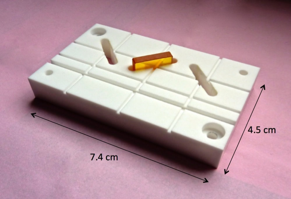
In collaboration with Prof Rob Lamb and Dr Ian Elder of Leonardo, Edinburgh, a hollow waveguide integrated optic mid-IR beam combiner has been designed, manufactured and assessed. As shown in the photograph, the beam combiner circuit is based on using 1.0 mm square cross-section hollow waveguides formed in a dielectric substrate to guide four different input wavelengths: 2.1 μm, 3.95 μm, 4.05 μm and 4.6 μm, to a single hollow waveguide output port. The wavelength combination process is achieved by means of three integrated dichroic components. The photo shows the circuit with one of the dichroic components located in its alignment slot. A lid forms the fourth (upper) wall of all the square section hollow waveguides. The approach has led to a compact, rugged, beam combiner with excellent optical performance and with the potential for quality controlled mass production. The work was funded by Leonardo, Edinburgh. |
9.7 μm Laser Heterodyne Radiometer
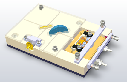
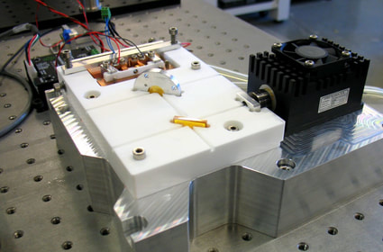
Above left and right respectively, are the isometric CAD design and the actual Laser Heterodyne Radiometer developed in collaboration with Dr Damien Weidmann (RAL Space, MIRICO) under funding from the Centre for Earth Observation Instrumentation CEOI (Director Mick Johnson). The system was design to operate in conjunction with a tunable 9.7 μm Quantum Cascade Laser local oscillator. As illustrated in the CAD design above, a lid (which is fixed to the top of the substrate) forms the upper walls of all the hollow waveguides in the optical circuit. The hollow waveguides take the form of square section channels in conjunction with the lid - thus forming square-section, hollow waveguides. Waveguides of this form are often referred to as "substrate integrated hollow waveguides". The performance of the radiometer far exceeded that of its free-space counter-part and was realised in a much more compact, rugged format.
Above left and right respectively, are the isometric CAD design and the actual Laser Heterodyne Radiometer developed in collaboration with Dr Damien Weidmann (RAL Space, MIRICO) under funding from the Centre for Earth Observation Instrumentation CEOI (Director Mick Johnson). The system was design to operate in conjunction with a tunable 9.7 μm Quantum Cascade Laser local oscillator. As illustrated in the CAD design above, a lid (which is fixed to the top of the substrate) forms the upper walls of all the hollow waveguides in the optical circuit. The hollow waveguides take the form of square section channels in conjunction with the lid - thus forming square-section, hollow waveguides. Waveguides of this form are often referred to as "substrate integrated hollow waveguides". The performance of the radiometer far exceeded that of its free-space counter-part and was realised in a much more compact, rugged format.
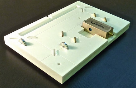
Differential Absorption Lidar for Atmospheric CO2 Monitoring
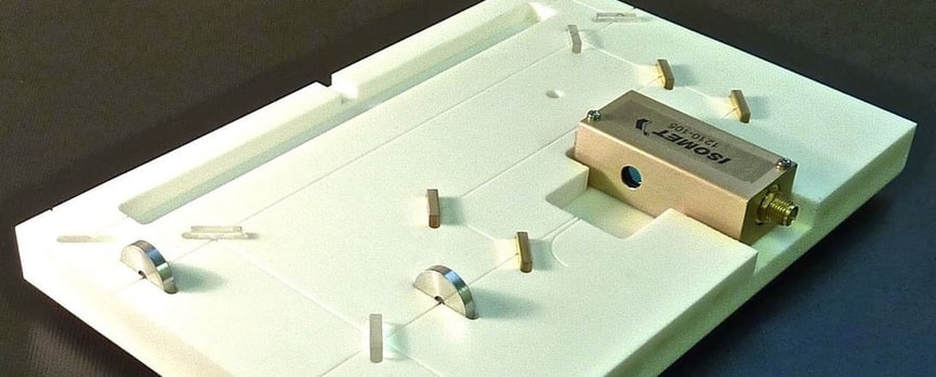
This is a photo of a 2.1 μm Differential Absorption Lidar (DIAL) demonstrator developed under research funding from the Centre for Earth Observation Instrumentation (CEOI) in collaboration with Prof. Roland Leigh University of Leicester . The DIAL system includes a range of optical components which facilitates coherent detection of return signals. The inclusion of an acoustic-optic modulator facilitates a frequency offset local oscillator function. Successful laboratory demonstrations (undertaken by Dr Brian Perrett, QinetiQ) served as a precursor for use in atmospheric CO2 monitoring. Following its conceptual design full engineering drawings for the baseplate, hollow waveguide substrate and lid were produced. The resulting STP files formed the basis of CNC milling programs for mass manufacture with a precision multi-axis milling machines such as a KERN Pyramid Nano.
This is a photo of a 2.1 μm Differential Absorption Lidar (DIAL) demonstrator developed under research funding from the Centre for Earth Observation Instrumentation (CEOI) in collaboration with Prof. Roland Leigh University of Leicester . The DIAL system includes a range of optical components which facilitates coherent detection of return signals. The inclusion of an acoustic-optic modulator facilitates a frequency offset local oscillator function. Successful laboratory demonstrations (undertaken by Dr Brian Perrett, QinetiQ) served as a precursor for use in atmospheric CO2 monitoring. Following its conceptual design full engineering drawings for the baseplate, hollow waveguide substrate and lid were produced. The resulting STP files formed the basis of CNC milling programs for mass manufacture with a precision multi-axis milling machines such as a KERN Pyramid Nano.
See also HollowGuide Ltd plus.google.com/101610815716104400462
